Microcomputer with AT89C51
Microcomputer based on Atmel AT89C51AC3
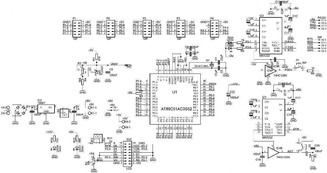
ELC8951 is a microcontroller system designed for general purpose, economical and highly expandable. It is based on the ATMEL AT89C51AC3 single-chip Flash microcontroller. The main features and hardware resources of the board are:
- Main clock frequency 29.4912 MHz
- 64 Kilobytes of downloadable flash memory that can be reprogrammed into the system
- 256 bytes of IRAM
- 2048 bytes of ERAM
- Serial EEPROM 2048 bytes
- 4-level 9-source breaks
- Array of counters programmable with
- High speed output
- Comparison / Capture
- Pulse width modulator
- Three 16-bit timers / counters
- Advanced programmable UART serial channel
- SPI serial interface
- Programmable watchdog timer
- 5 8-bit I / O ports
- 40 generic I / O pins
- RS232 serial port connector for in-circuit programming and data communications
- 8-channel 10-bit ADC with built-in 3,000V voltage reference source
- Double row 14-pin LCD connector (with trimmer contrast adjustment for LCD)
- 5 10-pin IDC connectors for cards and peripheral devices
- In-circuit programming of the main Flash micro-controller via the RS232 serial port
- On-board 5-volt linear regulator
- 12 V presence LED, 5 V presence LED, RS232 TXD and RXD activity LED
- 12 V DC power supply (6 to 12 V DC power sources can be used) or 5 V DC power supply
- Dimensions of 8.0 X 10.0 cm.
- 3.5mm mounting holes are on four corners.
- 0 ° - 70 ° C in operation, -40 ° - + 85 ° C storage temperature range.
The Flash microcontroller can be programmed via serial line even while in the final application circuit. Customers can program the microcontroller with the latest or customized firmware. This FLASH micro-controller feature makes it easy to develop and debug new programs. Downloading a program to the microcontroller usually takes a few seconds.
The well-known BASCOM51 and the SDCC development systems based on the ELCOSYS Micro-IDE integrated development environment, fully support programming and debugging within the system on the ELC8951 board using the serial port. There is also the Reads51 IDE available online.
A Windows-based ATMEL FLIP program is also provided to easily download programs to the card.
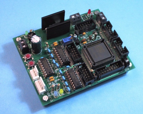
Board Layout
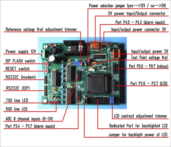
- 1 screw connector for 7 to 12 V power input (X4).
- 1 screw connector for 5VDC power supply input / output (X1)
- 1 screw connector for 5VDC power supply input / output (X6)
- 1 x 2-pin connector for 5V DC power input (X5)
- 1 power supply selection jumper, closed = 7… ..12VDC, open = 5V (JP1)
- 1 RESET switch (S2) for general microcontroller hardware reset
- 1 PSEN switch (S1) for manual activation of Flash programming mode.
- 1 x 4-pin Molex RS232C connector for general communication purposes (X2).
- 1 ISP RS232C 5-pin Molex connector for automatic software download
- 1 blue LED for monitoring the TXD ELC8951 line of the RS232 port (LED2).
- 1 yellow LED for monitoring the RXD ELC8951 line of the RS232 port (LED3).
- 1 trimmer for adjusting the reference voltage at 3.00 V (R3).
- 1 test point for measuring the reference voltage (TP1).
- 1 trimmer for adjusting the LCD contrast (R2).
- 5 10-pin IDC connectors signaled to the microcontroller I / O ports (P0, P1, P2, P3, P4)
- 1 x 16-pin IDC connector reserved for the LED backlit LCD module.
- 4. Parallel I / O ports pin-out and functional descriptionThe following notes describe the functions performed by each line of the five 8-bit parallel ports of the microcontroller referred to the pin-out of the IDC connectors. When a line is multifunctional, each different function is separated by a comma.Port 0 - IDC P0 connectorPort 0 is an 8-bit open drain bidirectional I / O port. Port 0 pins that have 1 written on them are movable and can be used as high impedance inputs in this state. Port 0 is also the low-order multiplex address and the data bus when accessing the external program and data memory. In this application it uses strong internal pull-ups when issuing 1. Port 0 also outputs Byte code during program validation. External pull-ups are required during program verification.Pin 1 = P0.0 Open-Drain bidirectional I / O linePin 2 = P0.1 Open-Drain bidirectional I / O linePin 3 = P0.2 Open-Drain bidirectional I / O linePin 4 = P0.3 Open-Drain bidirectional I / O linePin 5 = P0.4 Open-Drain bidirectional I / O linePin 6 = P0.5 bidirectional Open-Drain I / O linePin 7 = P0.6 Open-Drain bidirectional I / O linePin 8 = P0.7 bidirectional Open-Drain I / O linePin 9 = + 5V reference linePin 10 = GND reference linePort 1 - IDC P1 connectorPort 1 is an 8-bit bi-directional I / O port with internal pull-ups. Pins of port 1 can be used for digital input / output or as analog inputs for the digital to analog converter (ADC) in the 0-3 V range with voltage reference on the board. The port 1 pins that have written 1 are held high by the internal pull-up transistors and can be used as inputs in this state. As an input, the port 1 pins that are kept low externally will be the current source (IIL, see "Electrical Characteristics" section) due to internal pull-ups. The port 1 pins are assigned to be used as analog inputs via the ADCCF register (in this case the internal pull-ups are disconnected). As a secondary digital function, port 1 contains the Timer 2 external trigger and clock input; PCA external clock input and PCA module I / O. Port 1 receives the low order address byte during EPROM programming and program verification. It can drive CMOS inputs without external pull-ups.Pin 1 = P1.0 AN0: analog input channel 0, external clock input for Timer / counter2.Pin 2 = P1.1 AN1: Analog input channel 1, Trigger input for Timer / counter2.Pin 3 = P1.2 AN2: analogue input channel 2, external clock input PCA.Pin 4 = P1.3 AN3: analog input channel 3, PWM input / output PCA 0 In module.Pin 5 = P1.4 AN4: analog input channel 4, PWM input / output PCA module 1 In.Pin 6 = P1.5 AN5: analog input channel 5, PWM input / output PCA 2 In module.Pin 7 = P1.6 AN6: analog input channel 6, PWM input / output PCA 3 In module.Pin 8 = P1.7 AN7: analog input channel 7, PWM input / output PCA module 4 In.Pin 9 = + 5V reference linePin 10 = GND reference line